Today was the last day of classes for the first week of COSMOS! The week passed by much quicker than I expected. Today started with a lecture from Professor Nowadnick about materials in phones and electronics. She first had us brainstorm materials that we knew were in phones, such as aluminum, glass, gold, copper, lithium, and most importantly, silicon.
Professor Nowadnick then segwayed into a quick review of electric current, voltage, atoms, and valence electrons before talking about semiconductors, which are materials which have conductivity that can be controlled, and how silicon can be used to make semiconductors. She explained that there are two types of semiconductors made of silicon: n-type and p-type. N-type semiconductors are made by adding atoms with 5 valence electrons, typically phosphorous, to silicon, and the extra electrons from the phosphorous are free to roam and can carry current. P-type semiconductors are made by combining atoms with 3 valence electrons, usually boron, creating “holes” where electrons are missing that act as positive charges and can carry current. I was initially surprised to find out that these semiconductors are practically useless unless you combine them, but after learning about how they’re used, it makes a bit more sense.
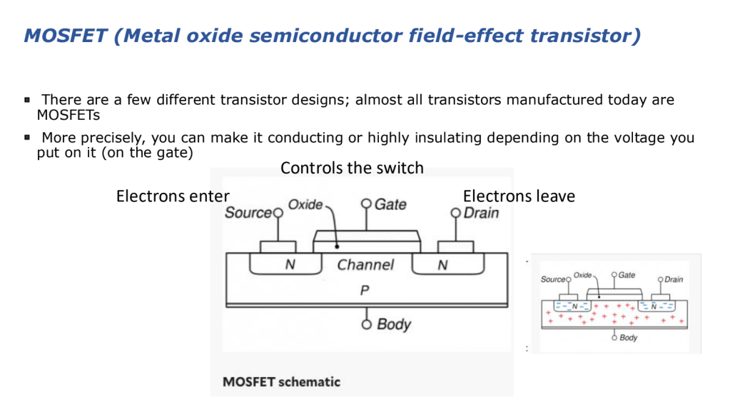
When one n-type and one p-type semiconductor are combined, positive and negative charges gather at a spot called the p-n junction, but the charges don’t have enough energy to jump across the barrier. When an outside energy source is connected (ex. a voltage), the electrons now have enough energy to flow across the junction, thus allowing current to flow. This is just my speculation, but since there is a build-up of charge, the current that flows is much stronger than if a regular conductor were to be used. This phenomenon is present in transistors, which have one n-type semiconductor, one p-type semiconductor, and a gate that we can control to allow current to flow through the channel. Below is a diagram of a transistor with its various parts labeled:
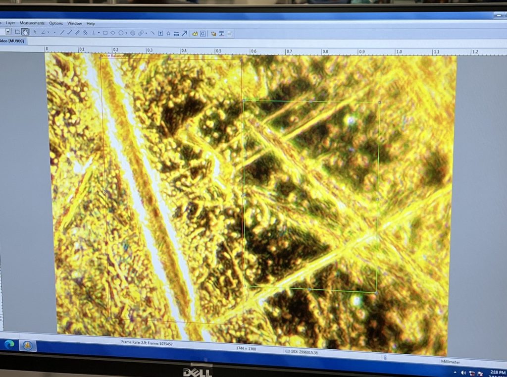
In the afternoon, we continued the lab from yesterday. After sanding and polishing our untreated and tempered samples, we got our samples etched by the graduate student TAs. Honestly, I’m not sure how etching works, so I’m going to have to brush up on it over the weekend. Then, we had to observe our samples under the microscope to look for the different phases in the steel.
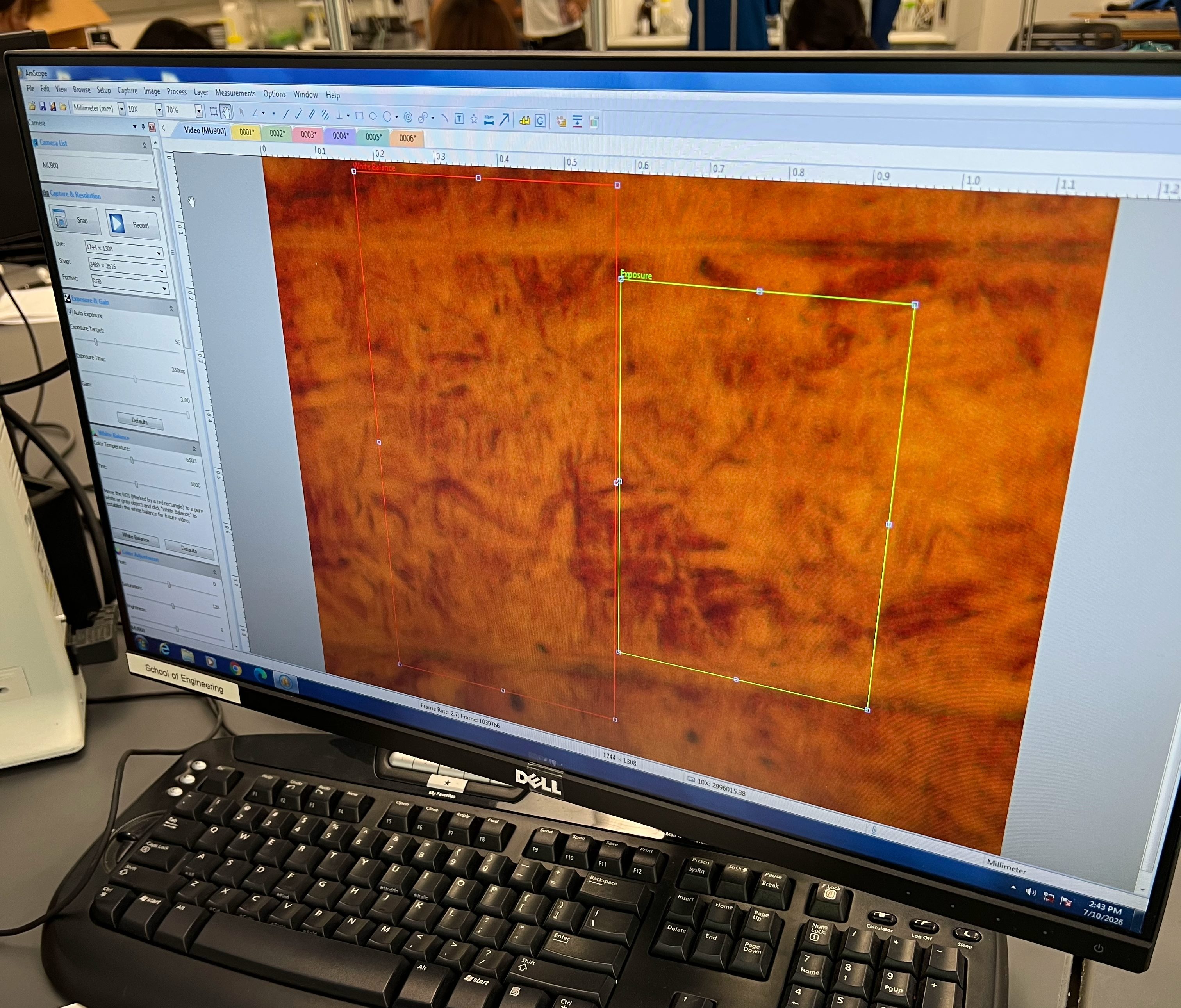
I know that the dark and light spots are two different phases, but beyond that, I don’t really know what I’m looking at. I’m also still unclear about why exactly two different colors show up—is it the austenitized steel trying to but failing at returning to its original form?


Leave a Reply